-
Notifications
You must be signed in to change notification settings - Fork 354
Memory Mapped Peripherals
Jeff Bush edited this page Jan 18, 2016
·
4 revisions
Peripheral registers can be accessed by reading and writing the memory region from 0xffff0000 - 0xffffffff. These must be 32-bit wide, aligned stores or loads. This mechanism allows adding communications peripherals like UARTs or internal accelerators.
These transfers control the following signals on the external core interface:
| Signal | Width | Description |
|---|---|---|
| write_en | 1 | Write enable |
| read_en | 1 | Read Enable |
| address | 32 | Read/Write address |
| write_data | 32 | Data to be written |
| read_data | 32 | Response to read request |
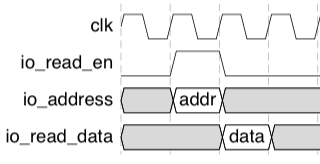
When a read is requested, the io_read_en signal is asserted along with the desired address. The peripheral must drive the result one cycle later. External logic must multiplex the read response based on the selected address.

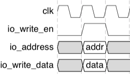
When a write is requested, the io_write_en signal is asserted with the desired address and data:
